Electronics repair
This is an introductory article on the repair of electronic items. While this is a broad and deep subject, this article aims to give some basic information that ought to get many failed electronic items up and running again.
Introduction
At one time there were an army of TV repair businesses and others that specialised in repair of electronic items. Alas due to the progress of technology, many of our electronic items have become far more sophisticated, and far more difficult to successfully diagnose and fix - especially without access to detailed technical information and elaborate test equipment. This coupled with ever lower prices for new equipment has resulted in the demise in large sections of the repair industry, and encouraged a "bin and replace" attitude among consumers. Unfortunately this often means that quite serviceable items with only minor faults are replaced when in reality replacement of a few discrete components often costing no more than pennies or just a few pounds would restore full operation.
Common Failures
Poor connections
One common failure is simply a poor connection - either due to wire damage inside the equipment, or more commonly a poor connection at a connector. Sometimes all that is required to fix an apparently faulty product is to unplug and remake an internal connection. The quickest way to find bad connections is to poke them with a plastic stick. Or use a multimeter on low resistance range, preferably one that has a buzzer or bleeper that indicates a good connection - test both ends of wiring for continuity.
Capacitors
Probably the single most common failure associated with modern digital electronics is that resulting from failed electrolytic capacitors, and in particular, failed capacitors in the power supply circuitry.
As these components age and begin to fail, they typically start to lose their capacitance, and this in turn tends to mean that power supply voltages either drift out of specified tolerance, or start to acquire excessive electrical noise or voltage ripple. Either of these will impair the operation of circuits powered by these supplies - often to the point of preventing something operating altogether.
Common failures of:
- LCD back lights in monitors and flat panel LCD TVs
- Power supplies for many modern bits of computer equipment, resulting in complete failure, or crashes and other unpredictable operation
- Power regulation circuitry on motherboards in computers, causing random reboots with no warning, system freezes, or simply a failure to start altogether.
- Power supplies in set top boxes, personal video recorders and other AV gear, causing random or unpredicted behaviour, missed recordings etc.
Can frequently be attributed to failing capacitors.
Diagnosis
Inspection
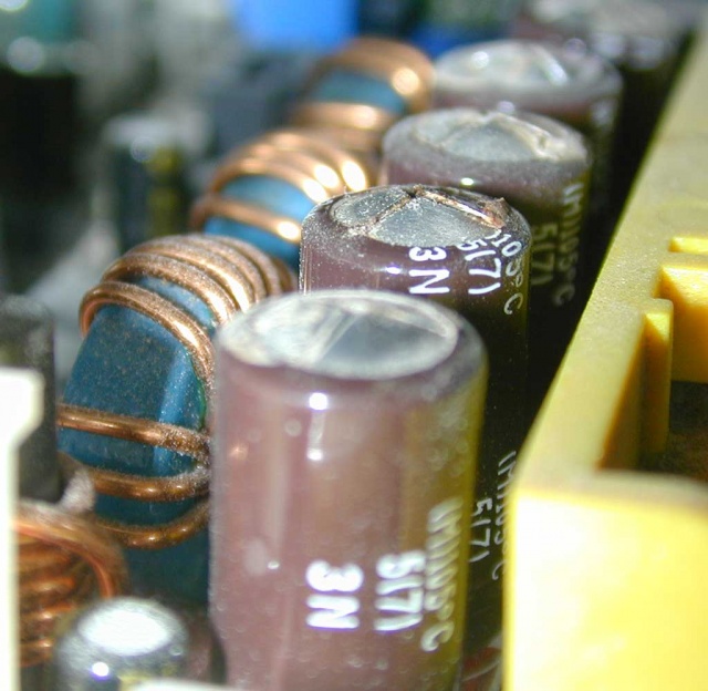
In some cases a visual inspection is all that is required to spot problem components. Look for signs of the top of the case bulging, or appearing dome shaped.
Failing CAP showing deformation and leakage from the top
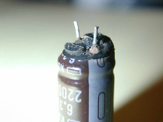
Any sign of leakage around the top or base. Or a component lifting from its base. If any of these faults are visible, then you can assume that even if not totally dead yet, they are not far from it.
Failed cap with base plug pushed out
ESR Meter
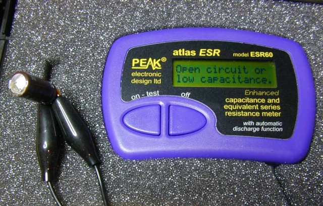
A very useful piece of test equipment for these devices is the Equivalent Series Resistance (ESR meter). These are rather specialised and are often dedicated to the one task, but they can give a very important reading of the overall health of a capacitor, that a reading of its capacitance alone will not give you. Often they can also be used on a device that is in circuit, meaning one can test devices without needing to remove them from the board first in many cases.
Typical ESR Table
| 10V | 16V | 25V | 35V | 63V | 160V | 250V | |
|---|---|---|---|---|---|---|---|
| 4.7µF | >40Ω | 35.0Ω | 29.0Ω | 24.0Ω | 19.0Ω | 16.0Ω | 13.0Ω |
| 10µF | 20.0Ω | 16.0Ω | 14.0Ω | 11.0Ω | 9.3Ω | 7.7Ω | 6.3Ω |
| 22µF | 9.0Ω | 7.5Ω | 6.2Ω | 5.1Ω | 4.2Ω | 3.5Ω | 2.9Ω |
| 47µF | 4.2Ω | 3.5Ω | 2.9Ω | 2.4Ω | 2.0Ω | 1.60Ω | 1.40Ω |
| l00µF | 2.0Ω | 1.60Ω | 1.40Ω | 1.10Ω | 0.93Ω | 0.77Ω | 0.63Ω |
| 220µF | 0.90Ω | 0.75Ω | 0.62Ω | 0.51Ω | 0.42Ω | 0.35Ω | 0.29Ω |
| 470µF | 0.42Ω | 0.35Ω | 0.29Ω | 0.24Ω | 0.20Ω | 0.16Ω | 0.13Ω |
| 1000µF | 0.20Ω | 0.16Ω | 0.14Ω | 0.11Ω | 0.09Ω | 0.08Ω | 0.06Ω |
| 2,200µF | 0.09Ω | 0.07Ω | 0.06Ω | 0.05Ω | 0.04Ω | 0.03Ω | 0.03Ω |
| 4,700µF | 0.04Ω | 0.03Ω | 0.03Ω | 0.02Ω | 0.02Ω | 0.02Ω | 0.01Ω |
| 10,000µF | 0.02Ω | 0.02Ω | 0.01Ω | 0.01Ω | 0.01Ω | 0.01Ω | 0.01Ω |
Note these are typical values for standard grade electrolytic capacitors at room temperature. please refer to manufacturers data sheets for specific values
Note also that lower values are generally better than higher ones. High quality capacitors may exhibit significantly lower values than those indicated above
Passive Component Testers
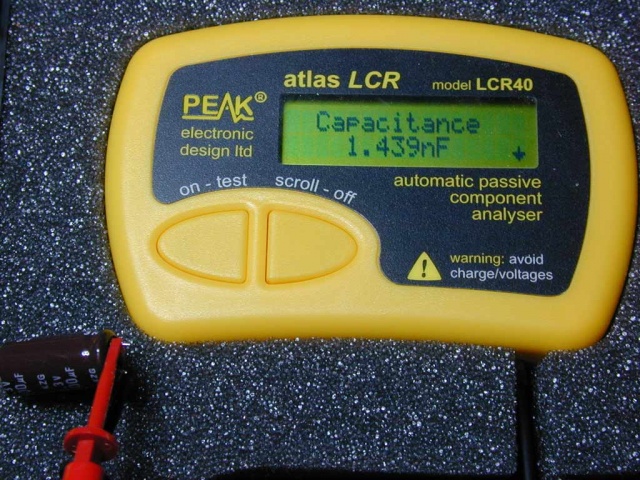
Passive component testers (aka LCR testers) are also useful. Now its possible to buy meters that do both jobs in one go.
Example of a failed cap which should have 2200uF of capacitance showing in effect none:
Multimeters
Many multimeters are also capable of reading larger values of capacitance - sometimes using one of the resistance ranges. Older analogue meters can be very useful since the characteristic "flick up" and decaying return of the needle as the capacitor charges up are good visual check on the functioning of the device.
In the absence of any test equipment or visible evidence, one can just go on the "replace anyway" principle. The parts are cheap, and sometimes its easier to just replace any likely candidates first and ask questions later!
Repair
Repair is simply a case of removing the existing device and substituting a similar one.
Choosing components
Replacement parts can be got new from electronic component sellers, or suitable parts can be removed from a wide range of scrap electronic equipment.
Ideally one should replace a device with one of the same capacitance, and the same or higher voltage rating.
If you can't find the exact capacitance, then in most cases its fine to use a larger value. How much larger depends entirely on the circuit, often one can double the value and its ok.
There's no harm is using a device with a higher voltage rating usually, a higher voltage device may be physically bigger and cost a bit more.
Caps of lower voltage rating should not be used. However having used them on occasion I've found they normally work fine. Popular electrolytic cap voltages are 6v, 10v, 16v, 25v, 35v, 50v, and when dropping one step down they're usually ok. If not, the thing fails dramatically right away - once it works it'll stay working.
When working on power supply circuits it is worthwhile choosing a good quality capacitor designed for "high ripple" operation and low ESR. Also look for one with a long quoted lifetime. Many of the better devices are quoted with a life of 10,000 hours. Some of the cheap ones are rated at 1,500 hours. For devices that stay powered and run for a long time (PVRs, set top boxes), this limited life can soon be swallowed in 18 months normal use.
If scavenging capacitors, I tend to pick 1980s equipment as first choice, as
- the caps are all modern types
- such kit often has more of them, for reasons beyond the scope of this article
- the caps are typically in better condition than post-90 goods
- The age of such caps is seldom an issue.
The picture on the right shows a filthy 1980s TV PCB cleaned up nicely by running it through a dishwasher.
Component replacement procedure
Component replacement requires that the equipment be disconnected from the mains, and stripped down enough to allow the offending circuit board to be accessed.
Having identified the components to replace it is worth noting (or photographing) their orientation to make sure you get the new ones back in the right way around. (sometimes there's printing on the board that identifies polarities and component numbers etc. Beware of neighbouring empty component positions, it can be unclear which position the component goes in once removed.
Desoldering
The principle of desoldering is simple, heat up the solder so it melts, then remove the component while the solder is liquid. Occasionally its useful to suck or mop the solder up while molten, but mostly not.
The reality can be more of a challenge sometimes.
Through hole removal
Simple passive components with two or three leads on single sided PCBs are usually straightforward to remove. You can either:
- its usually easiest to melt & rock - melt one solder pad and pull the component over to one side so the lead backs part way out of the hole. Repeat this going from side to side until its out. With diodes & transistors, let things cool down between melts.
- free one lead at a time in some cases
- melt both pads at once and pull the cap out - often needs a big soldering iron tip
The difficulty comes with multi leaded devices, and multilayer circuit boards.
Multi lead devices
These are more challenging as its difficult to melt all the connections at once.
- melt & rock can often be used, melting several legs at once.
- ICs etc are heat vulnerable, don't take longer than needed to melt, and always let them cool between melts
- Sometimes very little rock is possible, mainly by bending the PCB slightly, but any amount of movement will eventually get them out
- Solder removal techniques: some people use a sucker or braid to remove the solder. Success is variable, as partial removal makes it hard to melt what remains.
PCBs
The simplest PCB to desolder from is a single sided one (with tracks on only one side). Double sided boards with plated through holes are somewhat harder to desolder 'through hole' components from, as solder sit on both sides of the pin and also through the hole in the board, and fairly often one leg is soldered to a large area of copper that conducts heat away rapidly.
The hardest boards are multilayer ones as used in modern items with very high component integration densities like computers and other IT kit. Here the board design often has heavy copper power and ground plane layers sandwiched inside. These conduct the heat away from the soldering iron making reflowing the solder difficult.
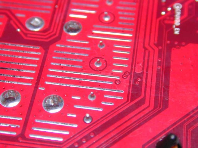
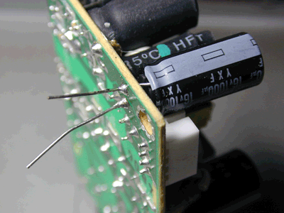
Here is an example of the rear of a computer motherboard, which has mostly surfaced mounted components. However the capacitors in the power regulation section are through hole, and pass through the board very close to (or soldered to) the heavy power and ground planes. (you can see the large expanse of copper track on the surface of this board)
When using a solder removal approach, when you remove most of the solder, it only takes a slight residue to keep a component firmly attached to a board. Removing solder removes the thermal conduction path to melt what remains, hence this approach is not first choice. The desire is to remove the device without doing any damage to the circuit board (damaging the component is usually ok, in most cases its defective)
Surface mount parts
The main methods are:
- Melt both ends at once: 2 irons or a large iron can take a lot of parts off in one go.
- Solder removal techniques: using a sucker or braid to remove the solder. Partial removal makes it harder to melt what remains.
- Barrier method: with surface mount ICs its often possible to melt the solder on some pins and slide a blunt razor blade or thin scalpel blade under them. Remove the blade once the solder is solid.
Equipment
- Soldering irons suited to desoldering usually have more power and bigger heavier tips fitted than those ideal for soldering.
- Solder suckers are very useful for clearing most of the solder from a joint, but poor quality suckers lack enough suck.
- Solder wick or braid can be very useful for cleaning remaining solder from a PCB once the component has been removed (very good on surface mount boards)
- Some liquid or paste flux is often handy to help the solder flow and make cleanup and removal simpler (especially with the wick / braid - a liberal application of flux, followed by heat applied to the top surface of the wick while its pressed against the board)
More specialist kit includes:
- desolder stations (big powerful soldering irons attached to a vacuum pump of some sort).
- Hot air solder stations (ideal for heating wider areas of a board at once soldering or desoldering multi lead devices in one hit)
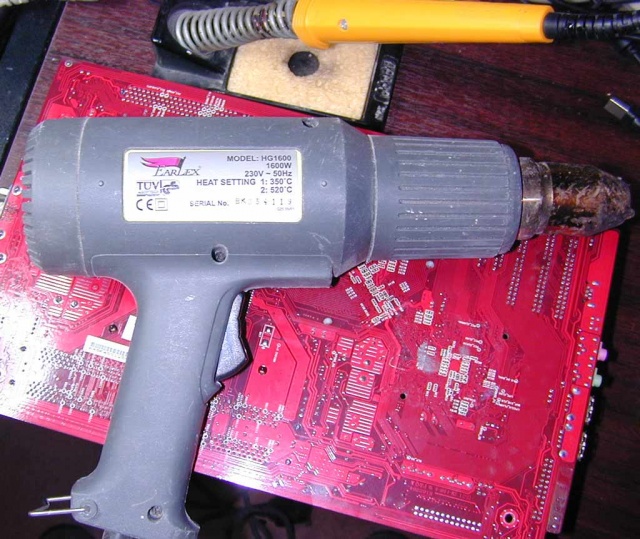
Although it sounds rather extreme, in the absence of a professional hot air station, there is a DIY tool that can be pressed into service here, and that is the heat gun:
This one has two temperatures, and the 350 deg C setting can be handy for getting enough heat into a multilayer board to bring it and all the layers up to a high enough temperature to reflow lead free solder. (note that you have little control and no finesse with this approach - it will get lots of heat into boards with substantial power planes like that pictured. However its really not the way to go if you are trying to do anything delicate with surface mount devices!)
Techniques
Small components with only a couple of connections can often be removed simply by melting the solder with a suitable iron, and pulling the device from the board while keeping the heat on. Take care not to apply too much force (especially force that would tend to push the solder pad away from the board surface). Using a large bit on the end of the iron can help supply enough heat.
Sometimes if the leads of the device are visible, cutting them to free the device is preferable, since the individual wires can be much simpler to remove individually. This can even work for surface mounted ICs with many visible legs. A sharp knife can be run down each side a few times to cut through the legs, and then each one individually flicked off with a hot iron.
In some cases, removing all the solder with a desolder tool will allow the component to be freed and removed (a gentle wiggle is sometimes needed to break the last grip of the remaining solder)
On multilayer circuit boards with through hole devices (like capacitors on a PC motherboard in the power regulator section) it can be very difficult to get enough heat onto the joints to reflow the solder - this is because the devices are often connected to heavy power planes on one of the inner "vias" on the board, and these suck the heat away too quickly. Here hot air solutions can work well since they can be used to preheat the surrounding area of the board and allow the area in question to be heated enough to melt the solder.
Modern electronics tends to use lead free solder. This is not only more problematic from a reliability point of view, it also needs a higher temperature to melt. It is often advisable to flux and apply more lead based solder to the joint first - this will mix with the lead free soder and tend to lower its melting point, making the subsequent reflow easier.
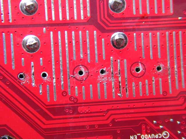
In this example of the PCB shown above, it was just about possible to remove the caps by heating each pin and turn and freeing it while the solder was molten using a normal soldering iron. However it was impossible to clear the solder from the holes to allow the new components to be inserted in this way. Hence hot air was used to heat the area of the board until the solder reflowed, and then a solder sucker applied to clear the hole. The other approach is to press the new leads into the holes once the solder in them is molten.
(most of the solder splatter on the red solder resist layer will wipe away, a hot iron and solder wick can be used for a final cleanup).
Not desoldering
Normally one desolders the defective part, but with only basic desoldering equipment it can be impossible to remove a cap from a multilayer board. In such cases its an option to leave the part in place. It leaves the risk of the failed capacitor leaking and damaging pcb tracks, but it generally works.
Insulated wire is soldered onto the pcb pads on the track side of the board, and the new cap soldered to the wires. Position the cap out of harm's way, and ensure nothing metal can touch the aluminium end of the cap, which is connected to the -ve lead.
If you need to glue the cap to stop it moving, acrylic or silicone work as long as they dry out fully before use. Cable ties, duct tape or hot melt adhesive are quicker. Double sided adhesive tabs generally fail.
Soldering
The basics of electronics soldering are pretty straight forward. As with all soldering be it pipes or components, the parts to join need to be immaculately clean and shiny, You need flux cored solder, and an appropriate soldering iron.
The fundamentals are:
- The metals to be jointed must be heated to above the melting point of the solder - you can't get solder to stick to (or "wet") metal that is cooler than the solder's melting point.
- the iron is held to the joint continually to do this, don't dab at it.
- Once existing solder begins to melt, apply solder to where the bit meets the joint.
- Once enough solder is on the joint, remove the solder wire. When the solder has spread across the joint, remove the iron. With transistors, diodes and chips don't keep the iron on longer than needed or the part can fry.
- Allow it to cool & solidify without any movement at all. It only takes a few seconds.
Its often advised to apply solder to the joint and not the iron when working on most "through hole" soldering and for soldering wires and terminals etc. This doesn't apply when working with surface mount boards, and when using separately applied flux. See the videos below:
Solder reflow
With electronic equipment, soldered connections can fail. This is often
- close to components that get hot (transformers, high power resistors, and high performance ICs etc). Thermal cycling can crack a soldered joint, creating a poor or intermittent connection.
- On heavy parts such as transformers
- On connectors that experience external strain
- On user controls
Reheating these joints and sometimes applying a little fresh solder repairs them.
With older lead soldered boards, you can often spot bad (or "dry") joints by their dull or misshapen appearance. Modern lead free solder has a greater tendency to fail in this way - again commonly near hot components.
Often, reflowing a whole IC with a hot air or IR rework station can fix problems.
Here is an example of a fairly simply reflow on a motherboard
(IR rework stations as shown, are around £160 on ebay)
Re-balling
The most difficult job to carry out is a reballing of a Ball Grid Array (BGA) component. This is a common package style for high performance ICs with very high integration levels that need to present many hundreds or even over a thousand separate connections to a circuit board, all in the space of a couple of square inches of physical space.
On modern motherboards (especially laptops) BGA packaged ICs can suffer solder joint failure. One way to identify these cases is where a device works when you apply mechanical pressure to the package (either directly or via a slight bend of the circuit board), and then stops working when you release the pressure.
Sometimes a simple reflow will also fix these, but it is often only a temporary solution. Although difficult, it is possible to do a proper DIY reball:
Note: the reballing stencils and holding frames can be had from eBay, starting at around £25 with one stencil.
When to re-ball
Reballing is often suggested for failing Graphical Processor Units (GPU) devices on motherboards. These can be prone to solder joint failure which is made more likely because many of the devices run very hot, and they are not always effectively cooled.
Note however there is also another common industry problem with certain ranges of GPUs that exhibited high failure rates due to internal failures of the device. These can confuse the situation since just heating the device alone will sometimes get it working again short term. Hence you can appear to have effected a repair by going through the reflow or re-ball process, when in fact the solder joint was not actually the cause of the problem in the first place. The "fix" was just a side effect of applying the heat required for the soldering operation. Alas these fixes are usually only short term, and the device will fail again in a few weeks or months.
When its not clear if this is the real issue, you can sometimes prove it by just reheating the device to a lower temperature that that required to actually reflow the solder - say 130 deg C. You may find that this will get it working again. If this works, then reflowing or reballing on its own will not fix the problem properly - the only real fix is to also replace the GPU with a new one (and make sure that its cooling is effective - proper contact with the heatsink, and good quality thermal transfer compound). Note on older devices, the ICs may not even be manufactured any more, which can make sourcing a replacement very difficult. Sometimes lifting a device from another scrapped board might be the only available source of a "new" device.
Example repairs
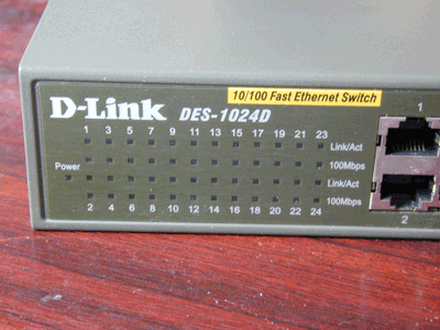
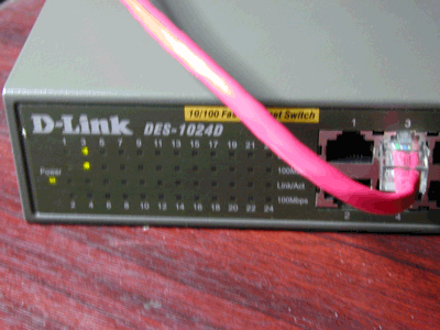
DLink DES-1024D & 1016D 10/100 Ethernet Switches
Two similar network switches, the 16 port displaying no signs of life at all, and the 24 port powered up, but would start to behave strangely and lock up once it had been in use for a while. The photos here show the diagnosis and repair for the 1024D, but the process was very similar for both.
Note these are mains powered devices, so take care to make sure its disconnected from the mains before work.
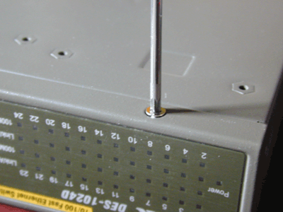
Opening is easy enough, flip over and remove the three screws from the underside front lip:
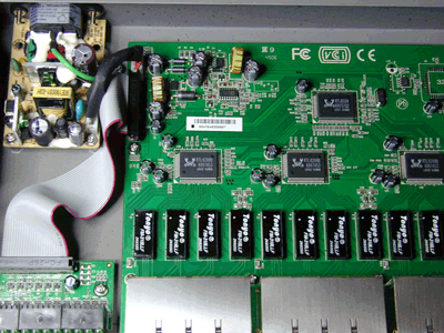
This reveals the main logic board, and the PSU board:
A visual inspection of the PSU board shows one suspect cap on the 24 port board, and a pair of them on the 16 port units PSU (similar but slightly different designs):
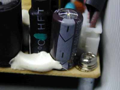
Taking the cap off board and checking, shows a capacitance around half the marked value of 680uF, a high ESR, and the device being identified as "leaky" by the ESR meter. Since the only spare to hand was a 16v 1000uF device, this was fitted in replacement - show here before the leads are clipped off:
The slight disadvantage to using the larger device here was that of physical space - it will not be possible to get the screw back into the right hand side of the board on the 24 port unit PSU as shown here (the layout of the PSU for the 16 port device was sufficiently different as to not have this problem, but then it had the screw missing from new anyway!)
A quick check with a volt meter shows a nice stable 5V output from the PSU, reassembled, and powered up:
Summary
A very quick and easy repair that could be done with zero test equipment and nothing more than a visual inspection if required. Total cost of replacement parts, under £1 per unit. Approx 10 mins work, and a pair of £40 - £60 devices kept out of landfill!
12V Sealed Lead Acid Battery Charger
A small 12V SLA battery charger that when powered up showed no apparent signs of life. The power and charge LEDs did not light, and there was no output voltage on the charge leads when measured on a multimeter.
Diagnosis
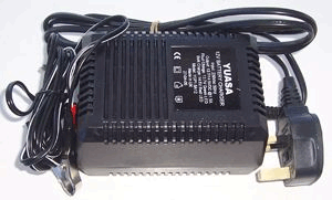
This was a reasonably heavy "brick" device not dissimilar to:
Using a resistance meter I first checked the fuse in the plug, that was ok. Since it probably had a conventional transformer connected directly to its mains input (the weight was a good clue), the next test was a resistance measurement between live and neutral pins on the plug to see if it was likely that the transformer primary had failed and gone open circuit (which given the price of a replacement would probably have made the charger beyond economic repair). However that showed a resistance of a few hundred ohms, so chances are it was ok.
Next take the lid off (four screws on the underside rather than a welded shut case, which was nice). That revealed a big transformer at one end of the case, and a small PCB at the other. The PCB contained among other things one dual in line IC in a socket - or at least partly in a socket! One end had lifted out (either the result of vibration or a knock on a hard surface) and half the pins were no longer making contact.
Fix
So, pushing the IC back into the socket, and powering up, showed it working normally again. Powered off and refixed the case lid. Job done.
Summary
Basically an example of a loose connection fault - even if socketed components are not obviously lose in their sockets, pushing them "home" can often work wonders. Total time to fix, under five minutes, and no cost for spares.
